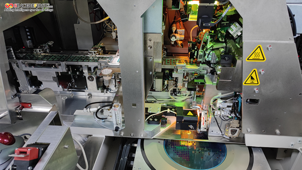
ie bonding is a manufacturing process used in the packaging of semiconductors. It is the act of attaching a die (or chip) to a substrate or package by epoxy or solder, also known as die placement or die attach. The process starts with picking a die from a wafer or waffle pack and then placing it at a specific location on the substrate. Die bonding requires high precision, reliability, and quality, as it affects the performance and functionality of the camera.
There are various methods of die bonding, such as soft solder, eutectic, epoxy, UV, silver sintering, thermocompression, and flip chip. Each method has its own advantages and disadvantages, depending on the application and requirements. Die bonding is an important step in the assembly of compact camera modules, which are widely used in smartphones, tablets, laptops, machine imaging and other Smart device.
Camera module die bonding is a process of attaching the camera sensor chip to the circuit board using an adhesive material. It is an important step in the assembly of compact camera modules, which are widely used in smartphones, tablets, laptops, machine imaging and other smart device Camera module die bonding requires high precision, reliability, and quality, as it affects the performance and functionality of the camera.


